


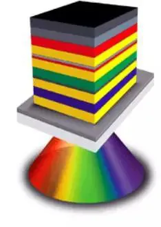
Color conversion method (light-color conversion method)
It is to add the center of energy transfer to the blue light-emitting layer, so that the short-wavelength, high-energy blue light can be converted into other colors of light by energy transfer. Therefore, it is easier to select materials and technology development, and only needs to be generated first. A blue light with excellent luminous efficiency and color purity, otherwise the overall luminous efficiency will be poor after energy conversion.
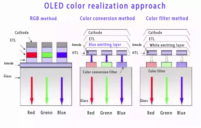
First, a device that emits white light or close to white light is prepared, and then through the tuning of the microcavity resonance structure, monochromatic light of different wavelengths is obtained, and then color display is obtained.
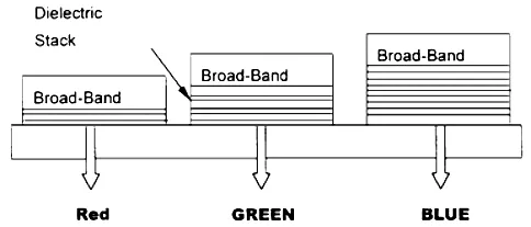
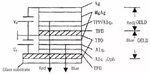
Adopt a stacked structure
Red, green, and blue light-emitting devices using transparent electrodes are stacked vertically to achieve color display.
OLED packaging technology
It is extremely sensitive to water and oxygen, so packaging technology directly affects the stability and life of the device.
Packaging technology
There are three main technologies:
Metal lid encapsulation, glass substrate encapsulation, thin film encapsulation.
Absorbent material
OLED devices have strict requirements for oxygen permeability.
There are two sources of moisture:
Penetrate into the device through the external environment;
Or the water vapor absorbed by each layer of material in the OLED process;
In order to reduce the entry of water vapor into the components or eliminate the water vapor absorbed by the process, generally the most commonly used substances are water-absorbing materials.
The desiccant and the desiccant sheet are attached to the inside of the encapsulating glass substrate to absorb the moisture inside the device.
Packaging process
The water and oxygen concentration control and the encapsulation process of encapsulating and pressing OLED devices must reach a certain standard and must be completed under the condition that the water and oxygen concentration is very low. The water oxygen concentration control is completed by the N2 circulating refining equipment. During the pressing process, it is necessary to control the height and width of the UV curing glue to make the pressure in the packaging chamber suitable to avoid the phenomenon of bubbles in the device after packaging.
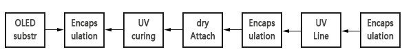
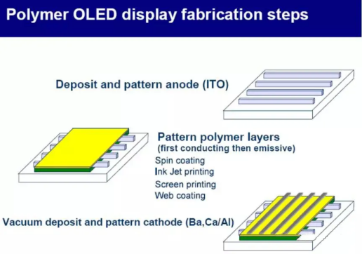
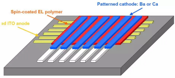
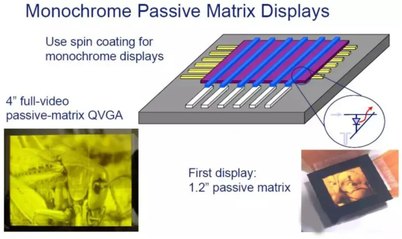
POLED preparation process
Spin coating
Dissolve the material in an organic solvent, drop it on the substrate, spin the glue, and evaporate the electrode. Simple, uniform film layer without pinholes, easy for large area devices
Spraying (int-jet)
Inkjet method to produce three primary color pixels, easy to achieve color and full-color display, simple process
Leaching method
Printing method
Device packaging
The organic materials and metal electrodes of the device undergo physical and chemical changes such as oxidation and crystallization when encountered with water vapor and oxygen, and thus fail. The device must be encapsulated, epoxy resin is encapsulated, and molecular sieve is added to absorb moisture.
OLED working characteristics
Luminous color
The characteristics of organic and polymer light-emitting colors:
The luminous color covers the entire wavelength range from ultraviolet to infrared. As long as the chemical structure of the chromophore or the type and position of the substituents on the chromophore are changed, the color control can be implemented; the color purity is poor. The absorption and emission spectra of organic and polymer are generally broadband spectra, and the half-height width of the peak is about 100~200nm. This is the result of the superposition of the vibrational energy level and the electronic energy level of organic molecules. Compared with inorganic luminescent materials, the color purity is much worse; the formation of radical-excited complexes and energy transfer occur.
OLED device efficiency
Internal quantum efficiency: the number of photons generated by exciton recombination / the number of injected electron-hole pairs
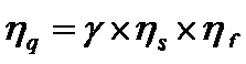
External quantum efficiency: the number of photons emitted from the device / the number of pairs of electrons and holes injected
From the working process of OLED, the external quantum efficiency can be expressed as
The main factors affecting the luminous efficiency of OLED:
Depends on the balance of charge injection.
In order to improve the quantum efficiency of the OLED, the number of holes injected into the organic light-emitting body from the anode should be equal to the number of electrons injected from the cathode.
Carrier mobility.
From injection to recombination, there is a migration and diffusion process in the direction of the electric field. In order to improve the efficiency of forming excitons, the mobility of positive load carriers should be large, and the difference between the two should be small.
Exciton radiation attenuation efficiency. The pH of organic light-emitting materials can reach 80% to 100%, while the pH of polymer light-emitting materials generally reaches about 20%.
Probability of singlet exciton formation.
Under normal circumstances, electrons are bound by holes, and 3 triplet excitons are generated at the same time for each singlet exciton. Therefore, even if the electrons injected into the device are all bound by holes, and all singlet excitons are radiated Generate photons, 25% will be the limit quantum efficiency of OLED. Because the transition of the triplet excitons is restricted by the law of quantum spin conservation, they cannot emit light, and 75% of the excitons are consumed in vain.
energy transfer.
When two chromophores coexist, the excited state of one chromophore can transfer energy to another chromophore to excite it. For the former excitons, this is “quenching”; for the latter chromophores, this is additional excitation, which greatly improves the luminous efficiency.
Measures to improve luminous efficiency:
1. Choose suitable electrode and organic layer materials to improve the efficiency and balance of carrier injection.
2. Adopt thin film structure and carrier transport layer to improve the mobility of two kinds of carriers, and make the difference between the two smaller.
3. Improve the interface characteristics of the device and increase the quantum efficiency of the device.
4. Use energy transfer to improve luminous efficiency.
5. Develop triplet electroluminescent materials.
Life and failure mechanism
The method of measuring the life of the component is to measure the time from the initial brightness to half of the brightness under the condition that the component maintains a constant current.
The best parameter for comparing lifetimes is the product of brightness and half-brightness lifetime. According to reports, the device with the longest service life of this value is: green light is 7000000 hr·cd/m2; blue light is 300,000 hr·cd/m2; red-orange is 1,600,000 hr·cd/m2.
The manifestations of the failure of OLEDs:
1. Under constant current working conditions, the brightness and efficiency gradually decrease.
2. OLEDs are stored in an atmospheric environment with a certain humidity and temperature for a certain period of time, and the brightness and efficiency of the luminescence will decrease until the luminescence disappears. This process reflects the storage life of OLEDs.
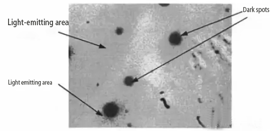
3. Regardless of whether it is storage or work, all failed OLEDs have a large number of non-luminous areas-dark spots.
OLED failure mechanism
Short circuit phenomenon
Because the organic film is not uniform and dense, there are micro conductive channels that penetrate the organic layer.
The formation of dark spots
1. Thermal effect-the thermal instability of the organic thin layer leads to the formation of black spots;
2. The chemical instability of organic polymer materials-organic molecules are easily corroded by oxygen and water and lose their ability to emit light;
3. The instability of the metal cathode-the metal cathode is oxidized;
4. The chemical reaction at the interface of the organic layer of the metal cathode-the electrochemical reaction of water, oxygen and aluminum will release a trace amount of gas, causing the metal cathode to peel off from the organic layer.
Impact of impurities
Impurities are the center of the non-radiative attenuation (heat generation) of trapped carriers and excitons, and can also cause local distortion of the internal electric field, which is an important reason for device aging and degradation.
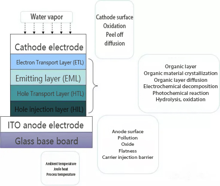
Decay of components
The decay of organic material components can be divided into three types:
1. Thermal decay. Tg can be used as a basis for its thermal stability. Materials with low Tg crystallize easily at room temperature.
2. Photochemical decay. Some organic materials are unstable under light irradiation and undergo photochemical reactions.
3. The interface is unstable. There are three kinds of interfaces in OLED devices: ITO/organic layer; organic layer/organic layer; metal/organic layer. Some organic materials have poor adhesion properties on other organic or inorganic materials.
The decay of inorganic material components can be divided into two types:
1. Surface contamination of ITO. The ITO surface in the device must be free of organic impurities. The leftovers on the surface will cause the operating voltage to rise, and the efficiency and service life will be reduced.
2. Corrosion of the cathode. Cathodic corrosion is the most common cause of device decay. If the package is not good, the device will appear oxidized black spots.
3. Life and failure mechanism
The control link to solve the life and stability problems of OLED devices
Control of ITO film quality and cleaning method
1. The choice of ITO glass
Leakage current at the anode interface and device stringing are closely related to the quality of the ITO film, which directly affects the life and stability of the device. The quality of the ITO film must be strictly controlled. Among them are the flatness, crystallinity, preferred orientation characteristics, grain size, grain boundary characteristics, surface carbon and oxygen content and energy level of the ITO film.
2. Preparation of ITO auxiliary electrode
When the manufacturer distinguishes the display screen, the ITO lines are too thin, and a metal auxiliary electrode needs to be added. The addition of the metal auxiliary electrode can reduce the resistance, facilitate the connection of the driving circuit, and improve the uniformity and stability of the light-emitting area.
When preparing the auxiliary electrode, the size of the square resistance, light transmittance, interface bonding characteristics, pattern etching characteristics, etc. should be considered.
3. ITO cleaning process
Contaminants on the ITO surface directly affect the efficiency, life and stability of the device. The pH value of the ITO etching solution, the cleaning and drying time and temperature, the parameters of UV cleaning and plasma cleaning, etc. should be systematically optimized.
Preparation conditions of isolation column
The photoresist, cleaning solution, rinsing conditions, drying temperature and time during the preparation of the isolation column have a greater impact on the life of ITO and the device. Optimizing the preparation conditions of the isolation column is the key to improving the stability and life of the device product.
Selection of stable OLED materials
Current hole transport materials with lower gas temperatures are a key factor. The low electron mobility of electron transport materials causes ineffective recombination, which directly and indirectly affects the life of the device. The choice of doping materials can effectively improve the efficiency and lifetime of the device.
Optimization of device structure
The energy level matching of each layer of the device, the control of the thickness of each layer, the control of the rate, the control of the doping concentration, especially the precise control and optimization of the thickness and rate of the cathode material LiF must be systematically optimized.
Optimization of packaging conditions
1. Control the temperature, humidity and cleanliness of the environment such as evaporation.
2. Preparation of pre-encapsulated multilayer film.
The test results show that the organic-inorganic multilayer film pre-encapsulated structure device has fewer aging black spots, and the stability and lifetime have been improved.
3. Encapsulate the desiccant. There are two ways to add encapsulated desiccant:
①Evaporate Ca0 and Ba0 desiccant films on the packaging glass;
② Paste Ca0 and Ba0 desiccants on the sealing glass.
These two methods are very effective for improving the life and stability of the device.
4. Packaging glue and its packaging method and the choice of packaging atmosphere. Encapsulation glue and UV packaging energy and temperature time directly affect the life and stability of the device, so the packaging glue and packaging conditions must be optimized. Different packaging atmospheres such as nitrogen and argon have a greater impact on the life and stability of the device. The current packaging technology is the key to controlling the life and stability of the device.
Connection condition
The uniformity of the connection and the size of the contact resistance affect the uniformity of the light emission of the device and the life of the device. Optimizing the connection material, heating temperature and connection time and other conditions are beneficial to improve the stability and life of the device.
Drive circuit(technical support)
The cross-winding of passive devices, reverse current and spikes seriously affect the stability and life of the device, research pulse width, duty cycle, reverse current, suppression voltage, circuit power consumption and screen power consumption, and constant voltage methods And the constant current method affects the life, optimizing the drive circuit is one of the methods to improve the life and stability of the device.